
Asia Pacific Semiconductor Ceramics Market Size, Competitive Landscape Analysis Report 2035
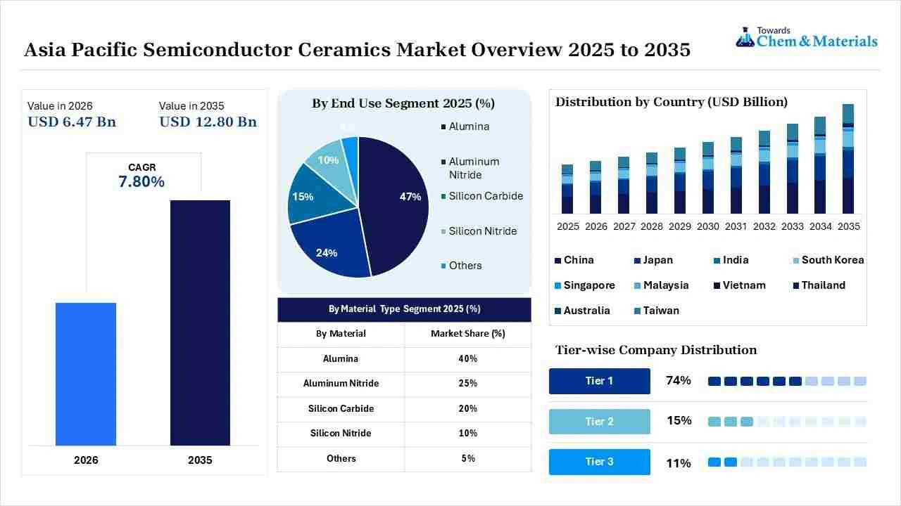
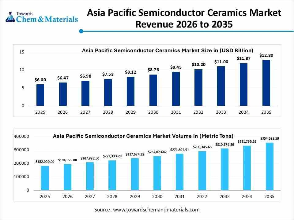
The Asia-Pacific semiconductor market size was valued at USD 6.00 billion in 2025, is estimated to reach USD 6.47 billion in 2026, and is projected to reach USD 12.80 billion by 2035, exhibiting a compound annual growth rate (CAGR) of 7.80% over the forecast period from 2026 to 2035.The Asia-Pacific semiconductor market is expanding due to large-scale global manufacturing, which supports a strong base for semiconductor, electronics, automotive, and power-device manufacturing. Countries such as China, Japan, South Korea, Taiwan, and India are increasing their production of chips and electronics. These materials are widely used around the globe because they can withstand high temperatures, provide electrical insulation, and improve heat management. As the world shifts toward AI and the adoption of smartphones, electric vehicles, 5G technology, and other high-tech devices accelerates, the production of semiconductor ceramics is increasing worldwide.
Key Takeaways
- By country, China dominated the Asia Pacific semiconductor ceramics market with a share of 34.00% in 2025 and is expected to grow at a CAGR of 8.04% in the forecast period.
- By region, Taiwan held 18.00% market share in 2025 and is expected to be the fastest-growing region in the market, with a CAGR of 9.10% in the forecast period.
- By material, the alumina segment dominated the Asia Pacific semiconductor ceramics market with a share of 47.00% and a CAGR of 6.90% in the forecast period
- By material, the aluminum nitrate segment held a 24% market share in 2025 and is expected to be the fastest-growing in the market, with a CAGR of 9.60% in the forecast period.
The Asia Pacific semiconductor ceramics industry is on the rise, which in turn is driving the growth of the semiconductor ceramic market in the region. Semiconductor ceramics are significant because they possess good heat resistance, electrical insulation, manufacturing durability, and stability. They are used in various applications of semiconductor manufacturing, such as equipment, substrates, and protective elements. There is growing demand for these materials in the production of electronic devices, electric vehicles, communication systems, and advanced chips. This is also due to the increasing emphasis on enhancing the performance of chips, lowering their heat output, and making electronic components smaller and more efficient.
- For instance, in May 2026, the Kyocera Corp took a step forward in the development of semiconductor ceramics, taking into consideration their capacity to improve performance and durability in electronic devices. As a result, these materials help enhance electrical insulation as well as heat resistance, backing up the growing demand in sectors such as automotive, communication, and high-tech industries, thereby contributing to the expansion of the ceramics market in Asia Pacific.
Global Investment Movement for the Asia Pacific Semiconductor Ceramics Market
- The increasing investment in manufacturing semiconductor ceramics and initiatives to set up plants across Asia Pacific are creating new opportunities for suppliers across the region. The investment to set up plants across the region is giving rise to new smartphones and high-tech products in the market, which is driving demand for this material to rise.
- The need for specialized ceramics is increasing as many companies are investing in manufacturing advanced product facilities, packaging units, and semiconductor equipment.
- Many countries across Asia Pacific, like China, Japan, South Korea, Taiwan, and India, are attracting significant investment into their semiconductor ecosystem.
- The demand for semiconductor ceramics is seen increasing in India as the country is heavily investing in chip fabrication, assembly, and packaging.
- There is growing interest in the use of high-performance ceramic materials, driven by the need for AI chips, electric vehicles, data centers, and other electronics.
- Investment is also shifting to advanced packaging, thermal management, and high-temperature components, and ceramics has an important role to play in these.
- Overall, the semiconductor ceramic market is forecast to witness robust growth in the semiconductor manufacturing sector, thereby offering favorable investment landscapes.
- For instance, in May 2026, NGK Corporation is planning to establish a new semiconductor plant in Japan with an investment of 4,200 crore rupees. This facility is expected to boost production capacity by 20%, facilitating mass production of semiconductor equipment by the year 2029. The decision to invest in the new plant is driven by the rising demand for AI technologies, smartphones, and data centers across the country.
- NGK To Invest ₹4,200 Crore In New Ishikawa Plant For Semiconductor Ceramics | Autocar Professional
- Countries, particularly in the Asia Pacific region, are channeling funds into infrastructure development to support manufacturing and distribution networks for semiconductor ceramics and related products. This includes upgrading facilities and transportation systems to improve supply chain efficiencies.
Report Scope
| Report Attributes | Details |
| Market Size in 2026 | USD 6.47 Billion/ 194,558 Metric Tons |
| Expected Size in 2035 | USD 12.80 Billion/ 354,690 Metric Tons |
| Growth Rate | CAGR of 7.80% |
| Base Year of Estimation | 2025 |
| Forecast Period | 2025-2035 |
| Segment Covered | By Materials, By End User |
| Key Companies Profiled | 3M, CeramTec GmbH, CoorsTek Inc., Elan Technology, Elster GmbH, Morgan Advanced Materials, Ortech Ceramics, Saint-Gobain, KYOCERA Corporation, OC Oerlikon Management AG |
Recent Market Trends
- Heat Managing Mechanism: The need for heat management is increasing. As the power of semiconductor devices has been enhanced, so are the demands for materials to handle and dissipate heat. The application of semiconductor ceramics is becoming significant as they can operate reliably in high temperatures and challenging operating conditions.
- Increased use in advanced packaging: With the increasing complexity and size reductions of semiconductor components, producers are seeking materials that offer excellent insulation properties, durability, and heat control.
- This is driving growth in the use of ceramic materials in advanced packaging and related applications.
Increasing demand due to AI and high-performance electronics: Demand for semiconductor ceramics is growing as a result of the development of artificial intelligence, data centres, electric vehicles and high-performance computing. These technologies involve components that need to be capable of dealing with increased power and operation. - Development of Better Manufacturing Techniques: Manufacturers are now directing their efforts towards better processing, shaping and finishing methods, which can enhance the manufacture of ceramics. The enhancements are contributing to the creation of components that are more accurate, stronger and consistent, as well as enabling more specialised semiconductor applications.
Innovation Transforming Asia Pacific Semiconductor Ceramics
Semiconductor ceramics are being innovated to improve their performance and usefulness. The progress of miniaturization and power increase of electronic devices has made ceramic materials demand greater heat dissipation, electrical insulation, and mechanical properties. Manufacturers are thus working to develop materials and manufacturing processes that will meet the evolving needs. Improving the thermal characteristics of ceramics is one of the key areas of innovation.
Materials such as aluminum nitride are being considered for applications where efficient heat transfer is important. Improved thermal management can further safeguard sensitive semiconductor devices and increase the reliability of their operation. In another step toward improvement, ceramic substrates and packaging elements have improved. Modern chips are also very hot and demand materials that will insulate them and help expel any excess heat. Better ceramic designs can help in high-performance electronics such as communication devices, artificial intelligence, and electric vehicles.
Manufacturing has also become more and more precise. Manufacturers can create more complex designs and achieve better consistency and precision of ceramic parts using advanced shaping, enhanced heating methods, and specialized surface treatments. The enhancements can help to improve the yield and reliability of parts employed in semiconductor production. Overall, innovation is improving the efficiency, durability, precision, and adaptability of semiconductor ceramics. Their use in next-generation semiconductor and electronic applications is anticipated with continued advances in materials and manufacturing processes.Absolics, a semiconductor manufacturing company, is establishing a facility in Covington, Georgia, as part of the
- CHIPS Act initiative. The investment aims to bolster local job creation and enhance the U.S. semiconductor supply chain, supporting advancements in technology and fostering innovation in the semiconductor industry.(Source:www.nist.gov)
Key Technological Shifts and AI in the Asia Pacific Semiconductor Ceramics Market
AI gradually plays a vital role in the semiconductor ceramics industry. Manufacturers can use AI to analyse vast amounts of production and material information to find more suitable material combinations and optimise manufacturing processes. This can shorten the testing time and assist companies in creating heat-resistant, strong, and electrically conductive ceramics. AI can also aid in quality control and defect identification. During the production process, cameras and intelligent software can detect cracks, various surface defects, size deviations, and so on. This enables manufacturers to identify issues before they occur and minimise material waste. One of the other uses is predictive maintenance.
AI systems can track equipment and detect irregularities in equipment behaviour. This can help manufacturers anticipate and solve potential issues before they disrupt their production. Even the development of AI is opening up opportunities for semiconductors based on ceramics. Due to the high power levels of AI processors and data-centre equipment, efficient heat management is essential. Ceramic materials can be utilized to help insulate and control temperature in such systems. AI is shaping the semiconductor ceramics industry on several fronts, from streamlining manufacturing processes to enhancing the capabilities of electronic devices.
As AI becomes increasingly integral to the semiconductor industry, so do advanced ceramic materials. Japanese ceramic companies are capitalizing on increased orders for specialised parts that are applied to chip manufacturing. One such application is the electrostatic chuck, a device that is used to firmly grip semiconductor wafers during manufacturing operations like etching. All these components must be capable of resisting high heat, plasma, and other corrosive conditions, which is crucial for the use of high-quality ceramics. Increasing production of memory chips, AI processors, and data-centre equipment is further supporting demand for these products.
- As the country specializes in making precision ceramics, the manufacturers are well suited for providing parts to high-tech semiconductor equipment. Meanwhile, increasing semiconductor manufacturing in Asia Pacific (APAC) markets is opening up new opportunities in the supply chain. The development highlights the impact of the swift rise of AI on both chip makers and those creating specific materials and components. With the rapid development of semiconductor technology, the market demand for high-precision, high-temperature-resistant, and reliable ceramic components will continue to rise.(Source:finance.biggo.com)
Supply Chain Analysis of the Asia Pacific Semiconductor Ceramics Market
Production & Processing
- In this process, materials are mixed, shaped, and treated according to their needs by controlling the heat resistance. The processing starts with the selection and preparation of appropriate raw materials, including alumina, aluminium nitride, and silicon nitride, depending on the use; these materials are mixed, shaped, and processed.
- The dimensions and quality are obtained by precision machining and surface finishing processes. Manufacturers are also turning to automated production processes to ensure accuracy, minimize defects, and ensure quality in the manufacturing of products.
- GlobalLogic, part of the Hitachi Group, has received a prestigious award from the Association for Talent Development (ATD) for 2026. This award is highly regarded worldwide and honors companies that use employee development to achieve business success. The recognition highlights GlobalLogics commitment to fostering a culture of ongoing learning through its innovative GlobalLogic Learning Experience (GLX) platform, which is designed to enhance employees skills and knowledge.(Source:www.globallogic.com)
- Key players: Absolics, AGC Electronic America, Air Liquide and Akash Systems
Quality Testing and Certification
- Semiconductors are manufactured in a very sensitive environment; quality testing is an important stage. Strength, thermal, electrical insulating, and dimensional properties, along with surface appearance and quality, are tested for products. Testing can also uncover cracks, impurities, and other factors that might ultimately impact performance.
- Manufacturers adhere to the proper quality standards and certification processes to produce products that meet the expectations of the semiconductor and electronics industry. Regular testing ensures reliability and minimizes failure risk in the industrial environment.
- In November 2025, a partnership deal was signed between STM International’s Additive Manufacturing Center of Excellence (AM CoE) and Additive Center B.V. (Eindhoven, Netherlands) to introduce additive manufacturing (AM) and quality assurance in the semiconductor industry. The aim is to ensure that all manufactured products are of good quality, will be used for years, and shall be of very good.
- ASTM & Additive Center Partner to Raise Quality and Certification in Semiconductor Sector - AM CoE
- Key players: BAE Systems, AGC Electronics America, Air Liquide and Akash Systems
Distribution to Industrial Users
- Shipping greener, lower-carbon materials to the manufacturing hubs across the countries to ensure a greener tomorrow. The industrial uses that are seen in the ongoing era are manufacturing units using reusable materials amid ongoing economic and geographical constraints.
- Products can be supplied directly from manufacturers, or via specialised distributors and regional suppliers.
- Most ceramic components need to be handled carefully and efficiently; this suggests packaging plays an important role
- From recent observations, Shyam Metallics has planned to invest rupees 2700 corer in a new project, which is aiming at increasing higher share margin in value-added steel products.
- Shyam Metalics and Energy Announces ₹2,700 Crore Capex Push for Specialty Steel Growth. | News On Project
- Key players: Corning, Edwards Vacuum, DuPont and EMD
Sustainability Analysis of Semiconductor Ceramics
Semiconductors are vital to a variety of todays technologies, such as smartphones, computers, electric vehicles, artificial intelligence, and communication systems. The production of semiconductors, however, consumes a lot of energy, water, and special chemicals, and sustainability is becoming a growing concern. The industry is thus striving to minimize its footprint and ensure the highest production standards. An essential objective is to increase manufacturing efficiency. Improved monitoring systems and AI technologies can assist manufacturers in detecting manufacturing issues, minimizing wasteful energy consumption, and optimizing the efficiency of the manufacturing process. Control of production conditions can also be used to reduce material and resource use, for example, when there is better control.
The industry is also looking for chemicals and gas alternatives that impact the environment less. Care must be taken to assess new materials and processes, ensuring they are safe for workers and reduce impacts on the environment. Another key area of interest is the design of semiconductors that are energy efficient. Cuts in energy use while using electronic equipment and data-centre hardware can be achieved by developing chips that consume less power. Manufacturers are also looking for opportunities to capture and utilise heat generated in the manufacturing process instead of letting it get wasted. Moreover, sustainability is gaining traction in the wider supply chain.
- For instance, in August 2026, India is focused on transforming its semiconductor ecosystem from ambition to execution, aiming to establish a sustainable supply chain. The government has initiated various incentives to attract foreign investment and enhance local manufacturing capabilities. Key objectives include promoting research and development, building fabrication units, and fostering collaboration between industries and academic institutions. With a rising demand for electronics and a shift towards greener technologies, India seeks to position itself as a key player in the global semiconductor market, ensuring resilience and self-reliance in this critical sector.
From ambition to execution: Indias path toward a sustainable semiconductor ecosystem
What are Semiconductor Ceramics?
Semiconductor ceramics are thin layers that are used for manufacturing products in AI, high-tech products, smartphones, and aircraft. This is also said to increase urbanization and industrialization, as governments are taking initiatives to set up new semiconductor plants across the country. An important factor that is contributing to higher demand is that this material controls heat and manages it very well. The price is also reasonable in Asia Pacific, which is making it easy to access for many firms around the region. The fact that sets it apart is minimizing rigid shapes by mixing all the materials; this makes the material very soft, making the transition smooth for manufacturing.
These kinds of materials are essential in the electronics industry for their ability to withstand demanding conditions and provide high-performance electronic components. The main reason why semiconductor is adopted because it prevents electric shocks and leakage, maintaining signal integrity. They are utilized for producing elements like wafer handling elements, ceramic substrates, components for insulation, electrostatic chucks, and other parts of the equipment. They are very useful in semiconductor fabrication because they are able to operate in high-temperature and chemically harsh environments. The materials need to deliver improved thermal performance and reliability as chips get smaller, faster, and more powerful.
Uses of Semiconductor Ceramics
Semiconductor ceramics are used widely, driven by their strength, heat resistance, electrical conductivity, and chemical resistance; semiconductor ceramics have a wide variety of applications. The main use is in semiconductor manufacturing equipment, where the ceramic parts are subjected to high temperatures and harsh processing conditions. They are applied to wafer-handling parts, chamber parts, insulating parts, and electrostatic chucks. For electronic and power devices, ceramic substrates are also employed as an electrical insulator and to control heat.
Materials that have high thermal characteristics are especially suited for use with high-power semiconductor components. Semiconductor ceramics are also employed in equipment for wafer processing, etching, deposition, and other manufacturing processes. They are used in electric vehicles, power electronics, telecommunications, artificial intelligence hardware, and equipment for data centers, in addition to traditional semiconductor production.
They are also highly resistant to degradation in harsh environments, making them ideal for use in high-performance electronic applications where long life and reliable performance are essential. Semiconductor ceramics are expected to be used for thermal management, advanced packaging, and high-performance electronic applications, which are becoming smaller and more powerful.
Pricing Analysis of Semiconductor Ceramics
Several factors dictate the pricing of semiconductor ceramics, such as ceramic type, purity, manufacturing complexity, and the component size and required performance. Basic ceramic components are typically much less costly than very specialized parts produced for semiconductor equipment.
The production of materials like aluminum nitride and silicon nitride can be more precise and require special processing, which can make them more expensive. High-temperature manufacturing also can increase manufacturing costs due to energy use. Further, ceramic components can also be surface-treated, polished, and/or machined to be more expensive for the end user. Semiconductor manufacturers, raw material availability, and production capacity can impact prices throughout the Asia Pacific market.
Sometimes large quantities of products can yield economies of scale advantages for the manufacturer, while highly customized parts are usually more costly due to the need for special designs and extra processing. Advanced chips, AI hardware, and EVs/PE can have a positive impact on pricing, especially for advanced ceramics. But better manufacturing efficiency, automation, and production volume may bring down costs in the future.
Asia-Pacific Semiconductor Ceramics Market Trade Analysis
Semiconductor ceramics are undergoing significant innovation to enhance their performance and applicability. As electronic devices become more compact and powerful, there is an increasing demand for ceramic materials that offer superior heat dissipation, electrical insulation, and mechanical properties. To meet these evolving requirements, manufacturers are focusing on the development of new materials and manufacturing processes. One key area of innovation is the improvement of the thermal characteristics of ceramics.
Materials like aluminum nitride are being explored for applications that require efficient heat transfer, which is crucial for protecting sensitive semiconductor devices and improving their reliability. Additionally, advancements in ceramic substrates and packaging have contributed to this progress. Modern chips operate at higher temperatures and therefore require materials that provide effective insulation and facilitate the dissipation of excess heat. Enhanced ceramic designs are vital for high-performance electronics, including communication devices, artificial intelligence systems, and electric vehicles. Manufacturing processes have also become increasingly precise.
Advanced shaping techniques, improved heating methods, and specialized surface treatments allow manufacturers to create more complex designs while achieving better consistency and precision in ceramic parts. These enhancements are expected to improve the yield and reliability of components used in semiconductor production. Overall, ongoing innovations are enhancing the efficiency, durability, precision, and adaptability of semiconductor ceramics. With continued advancements in materials and manufacturing processes, their role in next-generation semiconductor and electronic applications is anticipated to grow significantly.
Regulatory Framework: Semiconductor Ceramics Market
| Country Region | Regulatory Body | Key Regulations | Focus Areas |
| Asia Pacific | Ministry of Economy, Trade and Industry (Japan) | Export controls on critical materials and fab subsidization frameworks. | Securing raw materials from supply chains |
| North America | U.S. Department of Commerce (Bureau of Industry and Security); CHIPS Program Office | Export Administration Regulations (EAR) targeting advanced semiconductor components and ceramic substrates | Funding domestic materials for research. |
| European Union | European Commission; national authorities under the European Chips Act | Compliance for industrial manufacturing chemicals | Reducing import dependency for wafer fabrication equipment materials, enforcing stringent environmental and chemical safety standards |
Segmental Insights
Materials Insights
The alumina segment dominated the Asia Pacific semiconductor ceramics market with 47% market share and a 6.90% CAGR in the year 2025, due to its superior mechanical strength, electrical insulation, and heat resistance. It is used extensively in the manufacturing of semiconductor equipment, ceramic substrates, and insulating parts. It is also well-established in its manufacturing operations and has wide availability, which also contributes to its use for various applications. Alumina is preferred by semiconductor manufacturers for applications where reliability and cost-effectiveness are crucial. It has a solid track record throughout the semiconductor supply chain and is likely to hold its dominant place.
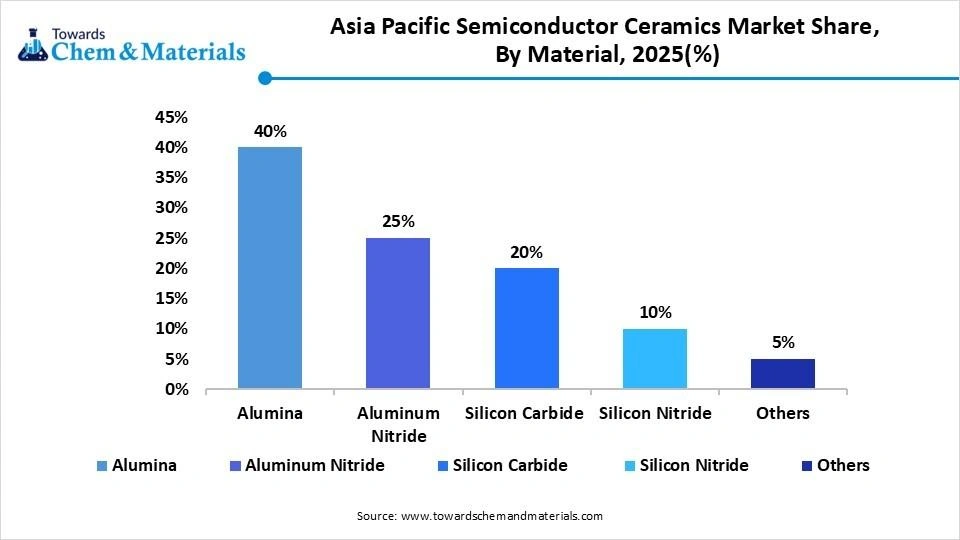
The aluminium nitride segment held a 24% market share in 2025 and is expected to grow at the fastest CAGR of 9.60% over the forecast period, as it is anticipated that aluminium nitride will be the fastest-growing material segment. Its high thermal conductivity allows it to be used in applications where heat removal is important. It also serves as electrical insulation, useful in the development of advanced electronic and semiconductor applications. Aluminium nitride is finding more applications for its growing use in AI processors, power electronics, electric vehicles and data-centre gear. The rising emphasis on advanced packaging and thermal management will aid its fast growth.
Asia Pacific Semiconductor Ceramics Market Share, By Material, 2025(%)
| By Material | Market Share (%) |
| Alumina | 40% |
| Aluminum Nitride | 25% |
| Silicon Carbide | 20% |
| Silicon Nitride | 10% |
| Others | 5% |
By end-user
The logic semiconductor chip segment dominated the Asia Pacific semiconductor ceramics market with a 45% market share and a 7.80% CAGR in the year 2025, driven by the capacity to operate high-tech devices. The demand for logic semiconductors is increasing in the market, followed by increasing adoption of smartphones, 5G internet speed, and requirements of artificial intelligence. As we say that mitochondria are the powerhouse of the cell, in the same way, a logic semiconductor chip is the brain of the central processing unit that let’s them read and process data very quickly. The main feature that keeps the demand for logic semiconductors high is their capacity, which enables the motherboard to perform complex tasks in a smooth and easy manner.
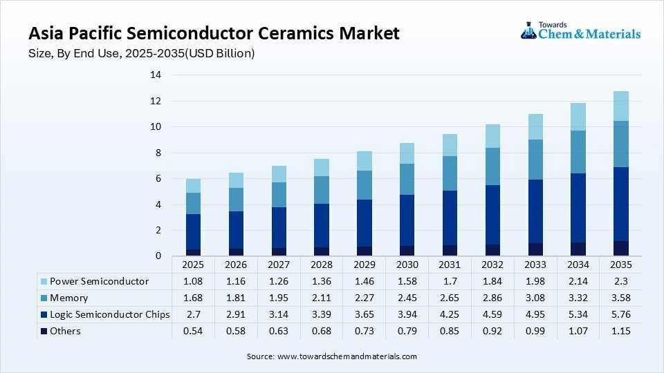
The memory segment held a 28% market share in 2025 and is expected to grow at the fastest CAGR of 9.01% over the forecast period, driven by the demand for manufacturing of the battery. If observed, then memory plays a very crucial role for a finished product in semiconductor ceramics. If we see then now a days many people, apart from asking about the features of a smartphones they, always go for what the memory of the phone is, along with another important question: what is the battery backup. This is where memory plays an important role. While manufacturing any high-tech devices like laptops, desktops, or mobile phones, memory is being extracted and increased so that the finished product can function smoothly for many long years, and this is what is making memory the most vital and booming factor in the semiconductor ceramics market. Also, the changing lifestyle of people is one of the key reasons why the need for memory is increasing.
Asia Pacific Semiconductor Ceramics Market Share, By End Use, 2025(%)
| By End Use | Market Share (%) |
| Alumina | 47% |
| Aluminum Nitride | 24% |
| Silicon Carbide | 15% |
| Silicon Nitride | 10% |
| Others | 4% |
Country Analysis
How Is Asia Pacific Contributing to the Semiconductor Ceramics Market?
The semiconductor industry and electronics and advanced manufacturing industries in Asia Pacific are key drivers of the semiconductor ceramics market. Several important semiconductor production centres are located in the region, such as China, Taiwan, Japan, South Korea, and India. Demand for Ceramic materials is being supported by increased investments in Chip manufacturing, electronic devices, Electric vehicles, and AI technologies. The area is likely to continue being a key growth area with the expansion of semiconductor production capacity.
China dominated the Asia Pacific semiconductor ceramics market with a share of 34.00% in 2025 and market size was estimated at USD 2.04 billion in 2025 and is projected to reach USD 4.42 billion by 2035, growing at a CAGR of 8.04% from 2026 to 2035., followed by a major electronics manufacturing base and a growing semiconductor industry.
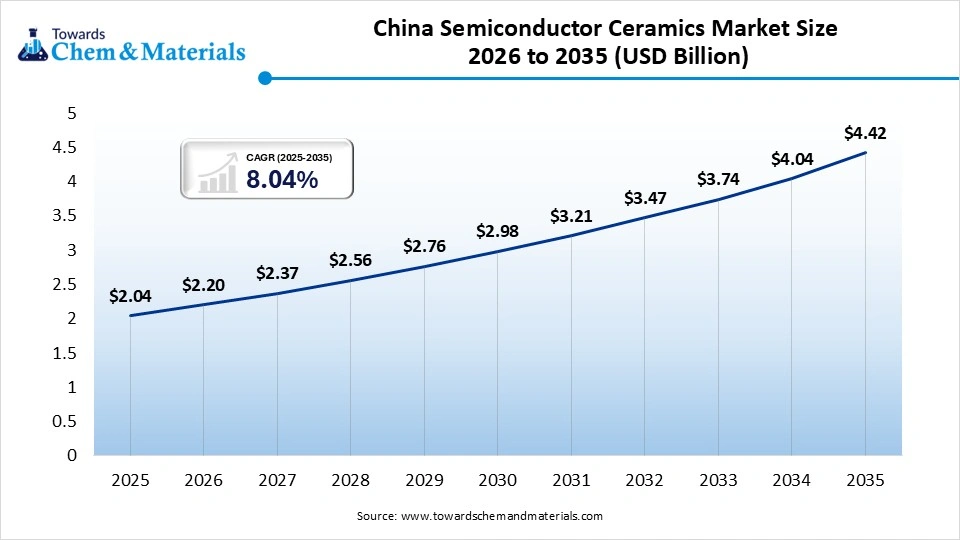
The country requires strong demand for ceramic components for semiconductor equipment, electronic devices, and power applications. Demand for specialised ceramic materials continues to grow with greater investment in domestic semiconductor manufacturing. New opportunities are arising in the expansion of EVs, consumer electronics, telecommunications, and AI-related infrastructure. China has a substantial industrial base and is increasingly moving towards localisation of semiconductors, which should help sustain its dominance in the market.
- For instance, in July 2026, China is strengthening its semiconductor industry by developing domestic deep ultraviolet (DUV) lithography technology. DUV equipment plays an important role in chip manufacturing and can be used to produce different types of semiconductor components. This development is particularly important as China faces restrictions on obtaining certain advanced chipmaking equipment from foreign suppliers. Building its own lithography capabilities could help the country reduce dependence on imported technology and improve its semiconductor supply chain. It may also support greater domestic chip production and strengthen China’s position in the global semiconductor industry.(Source:www.cnbc.com)
Taiwan held an 18% market share in 2025, and market size was estimated at USD 1.08 billion in 2025 and is projected to reach USD 2.37 billion by 2035, growing at a CAGR of 8.18% from 2026 to 2035, driven by a wealth of chip production and advanced manufacturing, and thus has constant demand for high-quality ceramic components. The demand for materials with increasingly superior thermal and electrical characteristics is rising with the growing production of advanced processors and complex semiconductor packages. The future will include more investment opportunities in advanced chip technologies and manufacturing capacity. Global semiconductors are an important growth market where Taiwan also has a strong position in global semiconductor production.
The Japan market size was estimated at USD 1.50 billion in 2025 and is projected to reach USD 3.26 billion by 2035, growing at a CAGR of 8.07% from 2026 to 2035. Japan has a long and rich history in advanced ceramics and precision manufacturing and is an important market for semiconductor ceramics. Japanese firms are well equipped to manufacture special ceramic materials and semiconductor equipment parts. The semiconductor equipment, electronics, automotive, and advanced technology sectors provide support for demand. The semiconductor industry is seeing an increase in investment, which is opening new opportunities for the ceramic industry. Demand in Japan should remain high in the future as high-performance electronic and semiconductor technologies continue to develop.
- For instance, in May 2026, NGK Corporation is planning to establish a new semiconductor plant in Japan with an investment of 4,200 crore rupees. This facility is expected to boost production capacity by 20%, facilitating mass production of semiconductor equipment by the year 2029. The decision to invest in the new plant is driven by the rising demand for AI technologies, smartphones, and data centers across the country.
NGK To Invest ₹4,200 Crore In New Ishikawa Plant For Semiconductor Ceramics | Autocar Professional
The India market size was estimated at USD 0.18 billion in 2025 and is projected to reach USD 0.45 billion by 2035, growing at a CAGR of 9.60% from 2026 to 2035.India is now becoming a potential market for semiconductor ceramics due to the growing indigenous semiconductor manufacturing industry. With the development of the domestic semiconductor manufacturing industry in India, the country is emerging as a promising market for semiconductor ceramics. The growth of investment in chip manufacturing, semiconductor packaging, and electronic manufacturing is anticipated to lead to further demand growth for ceramic components. The growth of electric vehicles, telecom, consumer electronics and digital infrastructure is also helping to create market opportunities. The government and private industry are making efforts to make the semiconductor supply chain more robust, which is driving more investment in the industry. With the improvement of its production ability, India is expected to be an increasingly important market for semiconductor ceramics.
The Australia market size was estimated at USD 0.02 billion in 2025 and is projected to reach USD 0.10 billion by 2035, growing at a CAGR of 17.46% from 2026 to 2035.The market for semiconductor ceramics in Australia is a small but growing market in the Asia Pacific region. It has benefitted from an increased interest in advanced technologies, electronics, research and specialised manufacturing. The countrys attention to building up more resilient technology and critical material supply chains can enable advanced ceramic applications. Demand is also likely to grow with Australias active expansion in renewable energy, electric mobility and high-performance electronic systems. Due to the limited size of the market compared to China, Taiwan or Japan, gradual growth of semiconductor ceramic applications can be achieved through continued technology development.
Recent Developments
- In August 2026, Jubilant Ingrevia plans to acquire a 40% stake in Zettaone Tech for ₹189.2 crore, aiming to enhance its presence in the semiconductor value chain. This strategic move aligns with the companys focus on expanding its portfolio and tapping into the growing demand for semiconductor technologies.
- Jubilant Ingrevia to acquire 40% stake in Zettaone Tech for Rs 189.2 crore; bets on semiconductor value-chain - Industry News | The Financial Express
- In august 2026, India is poised for a new deep-tech investment cycle, driven by the booming semiconductor and space technology sectors. As global demand for advanced technologies surges, local firms and startups is attracting significant funding, marking a transformative shift in the country’s innovation landscape and economic growth trajectory.
- Semiconductor and spacetech boom: Is India entering a new deep-tech investment cycle? | Stock Market News
Competitive Analysis
The Asia Pacific semiconductor ceramic market is highly competitive, and the firms are emphasizing product quality, precision, durability, thermal performance, and technological development. Japanese manufacturers are in a good position because of their expertise in ceramics, and they have established supply networks for semiconductors. To strengthen the semiconductor value chain and boost local industry competition, China is putting its muscles into its supply chain. Taiwan, South Korea, and Japan are still crucial markets due to their high-tech chip manufacturing capacities. There is a growing need for high-performance materials, like aluminum nitride and silicon carbide, that are being developed by companies to address thermal-management requirements. Research and development, production capacity, tailor-made solutions, and secure supply chains are driving competition in the region.
Top Players in the Market & Their Offeringss
| Company | Company Type/Position | Major Headquarters | Geographic Presence | Offerings | Key Strength |
| Absolics | Materials | Covington | Global | modernization | Manufacturing |
| AGC Electronic America | Materials | Hillsboro | U.S. | modernization | Manufacturing |
| Air Liquide | Materials | Phoenix | U.S. | modernization | Manufacturing |
Other Key Players
- 3M
- CeramTec GmbH
- CoorsTek Inc.
- Elan Technology
- Elster GmbH
- Morgan Advanced Materials
- Ortech Ceramics
- Saint-Gobain
- KYOCERA Corporation
- OC Oerlikon Management AG
Segment Covered in the Report
By Materials
- Alumina
- High-Purity Alumina
- 96% Alumina
- 99.5%+ Alumina
- Translucent Alumina
- Aluminum Nitride
- Standard AlN
- High-Thermal-Conductivity AlN
- High-Purity AlN
- Silicon Carbide
- Sintered SiC
- Reaction-Bonded SiC
- High-Purity SiC
- Silicon Nitride
- Reaction-Bonded Si₃N₄
- Hot-Pressed Si₃N₄
- Sintered Si₃N₄
- Others
- Beryllium Oxide
- Zirconia
- Mullite
- Cordierite
- Steatite
By End User
- Logic Semiconductor Chips
- Memory
- Power Semiconductor
- Others
By Contry
- China
- Japan
- India
- South Korea
- Taiwan
- Rest Of Asia Pacific
A Seven-Phase Framework
Our methodology is designed to be universally applicable across commodity chemicals, specialty chemicals, petrochemicals, construction chemicals, coatings, electronic chemicals, industrial gases, agrochemicals, water treatment chemicals, and performance materials. Each phase builds upon the last, creating a layered validation structure that minimizes estimation error and maximizes analytical confidence.
The framework ensures comprehensive market coverage, robust cross-validation, and reliable long-term forecasting — producing market estimates that withstand scrutiny from investors, regulators, and corporate strategy teams.

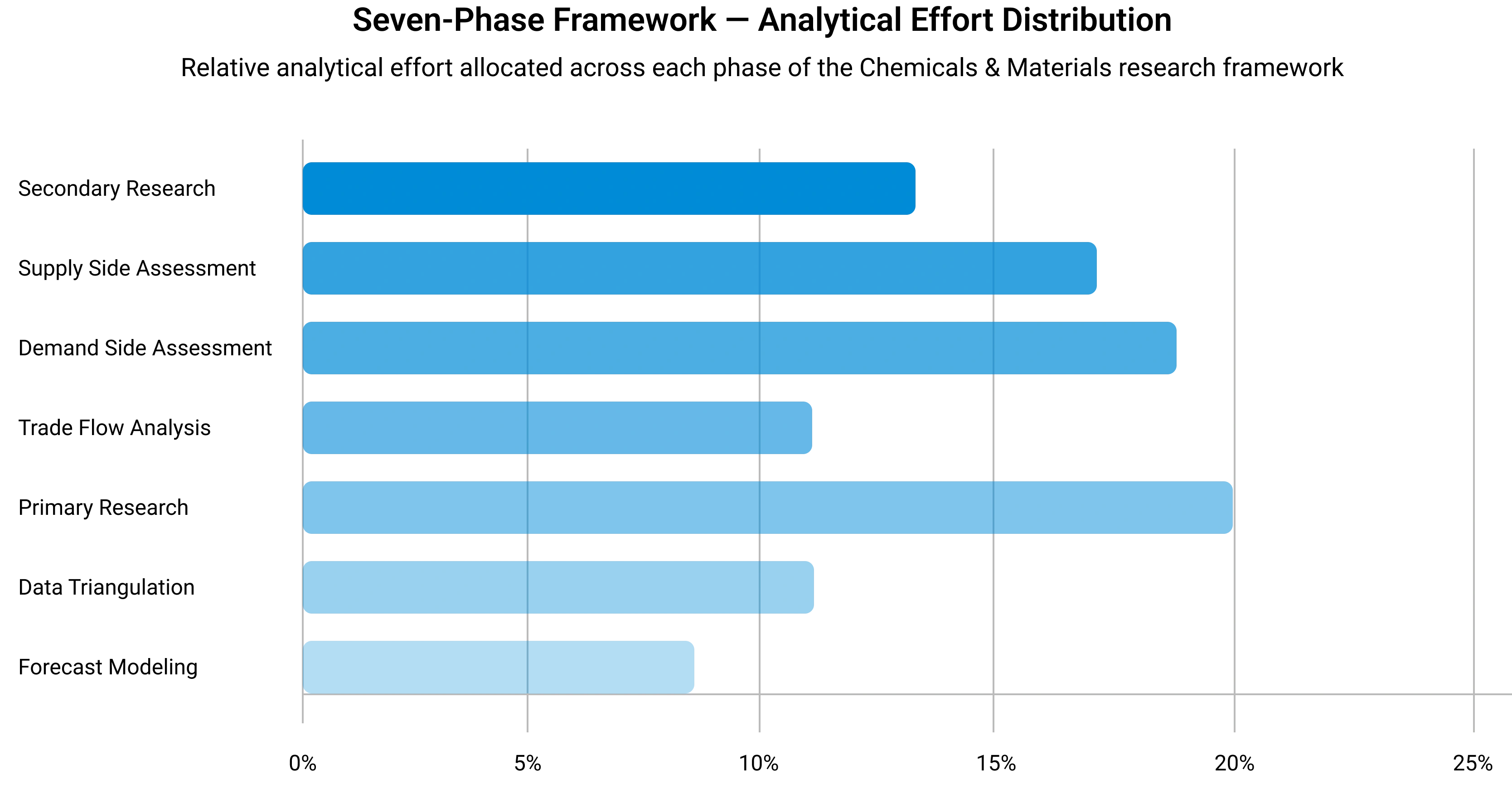
Seven-Phase Framework — Analytical Effort Distribution
Relative analytical effort allocated across each phase of the Chemicals & Materials research framework
Phase 1 - Secondary Research: Establishing the Foundation
Secondary research collects and evaluates publicly available information from authoritative sources, establishing the foundational understanding of market structure, value chain dynamics, competitive landscape, and end-use demand patterns. Every source is evaluated for credibility, recency, geographic relevance, and methodological soundness before inclusion.
Industry Associations
Sources include ACC, CEFIC, ICCA, JCIA, CPCIF, and SOCMA providing production volumes, consumption trends, capacity developments, and sustainability initiatives.
Company Disclosures
Annual reports, investor presentations, earnings transcripts, and regulatory filings reveal product portfolios, manufacturing footprints, capacity expansions, and revenue segmentation.
Government Databases
National statistical offices, customs authorities, environmental agencies, and industrial production databases provide verified statistics on output, trade flows, and regulatory compliance.
Trade Databases
UN Comtrade, ITC, Eurostat, and national customs authorities enable assessment of global product movement, import dependency, and export competitiveness across regions.
Our Secondary Research Sources
- Ministry of Chemicals and Fertilizers
- European Chemicals Agency
- United States Department of Energy
- Ministry of Industry and Information Technology
- Ministry of Economy Trade and Industry
- Ministry of Trade Industry and Energy
- National Institute of Standards and Technology
- Council of Scientific and Industrial Research
- Fraunhofer Society
- National Institute for Materials Science
Phase 2 — Supply-Side Assessment: Mapping Production Capabilities
Production Capacity Analysis
All major manufacturers are assessed for existing installed capacity, planned additions, expansions, new plant announcements, and technology adoption — mapped at global, regional, and country levels.
Capacity Utilization Adjustment
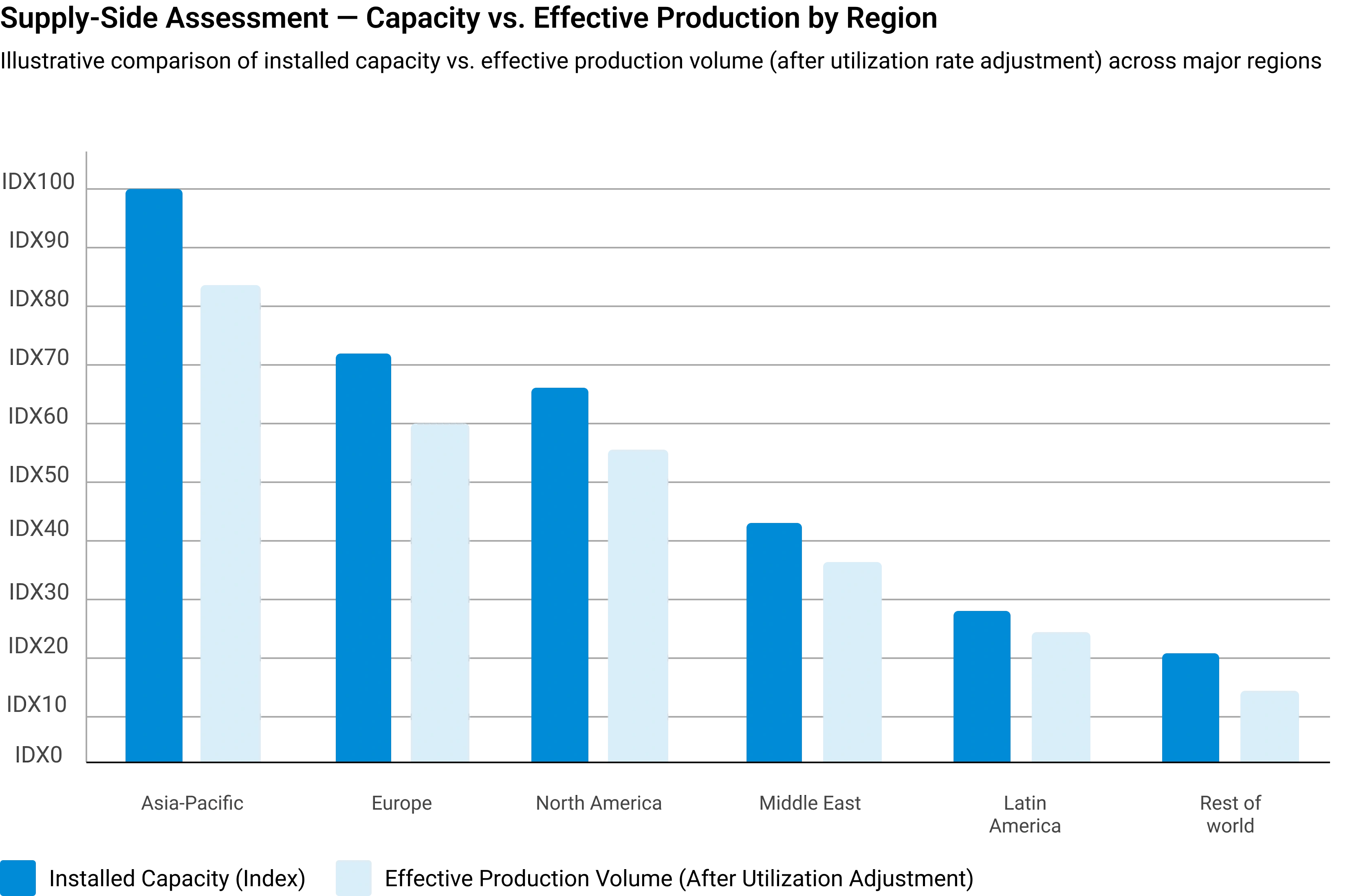
Installed capacity is adjusted using utilization rates based on demand conditions, feedstock availability, plant operating rates, maintenance schedules, and regulatory restrictions.
Manufacturer Revenue Analysis
Product-specific revenues, segment-level performance, regional distribution, average selling prices, and margin trends are evaluated to establish market value estimates.
Supply-Side Assessment — Capacity vs. Effective Production by Region
Illustrative comparison of installed capacity vs. effective production volume (after utilization rate adjustment) across major regions
Phase 3 — Demand-Side Assessment: Quantifying Chemical Consumption
Demand-side analysis quantifies chemical consumption across industries, applications, and geographies — identifying where and how chemicals are consumed throughout the value chain with precision.
End-Use Industry Analysis
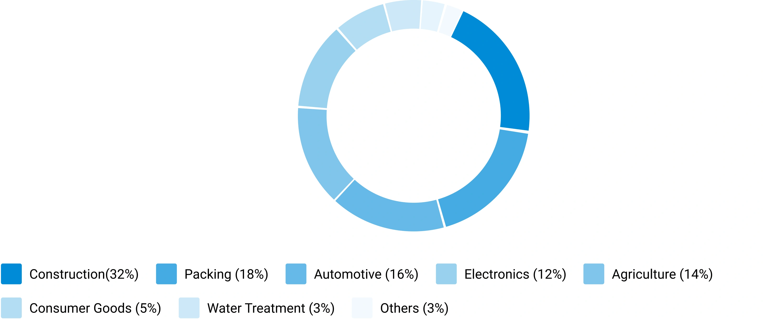
Chemical demand is evaluated across automotive, construction, packaging, electronics, agriculture, healthcare, consumer goods, industrial manufacturing, energy and utilities, and water treatment. Industry output, production trends, and consumption intensity are analyzed to determine demand patterns.
Consumption Modeling
Demand is estimated using measurable indicators: kilograms per vehicle, kilograms per square meter of construction, dosage per cubic meter of water treated, kilograms per hectare of agricultural land, and kilograms per ton of manufactured products. Consumption factors are validated through industry publications and primary interviews.
Application Analysis
The market is segmented by application area to understand product performance requirements, formulation trends, technology adoption, customer preferences, and regulatory requirements improving demand accuracy and segmentation granularity.
Demand-Side Assessment — End-Use Industry Demand Distribution
Illustrative distribution of chemical & materials demand across key end-use industries
Phase 4 - Trade Flow Analysis: Balancing Regional Supply and Demand
Trade flow analysis reconciles regional supply and demand estimates through import and export data, identifying net supply positions, regional dependencies, and market imbalances. It serves as an independent validation layer that tests the consistency of supply-side and demand-side estimates.
Import Analysis
Import data is evaluated to determine volumes, source countries, product dependency, regional supply gaps, and pricing trends — identifying markets that rely heavily on external supply and where domestic production is insufficient to meet demand.
Export Analysis
Export assessments reveal production surplus, export competitiveness, regional manufacturing strength, and global market participation. Export patterns also help validate domestic production estimates and identify net exporting regions.
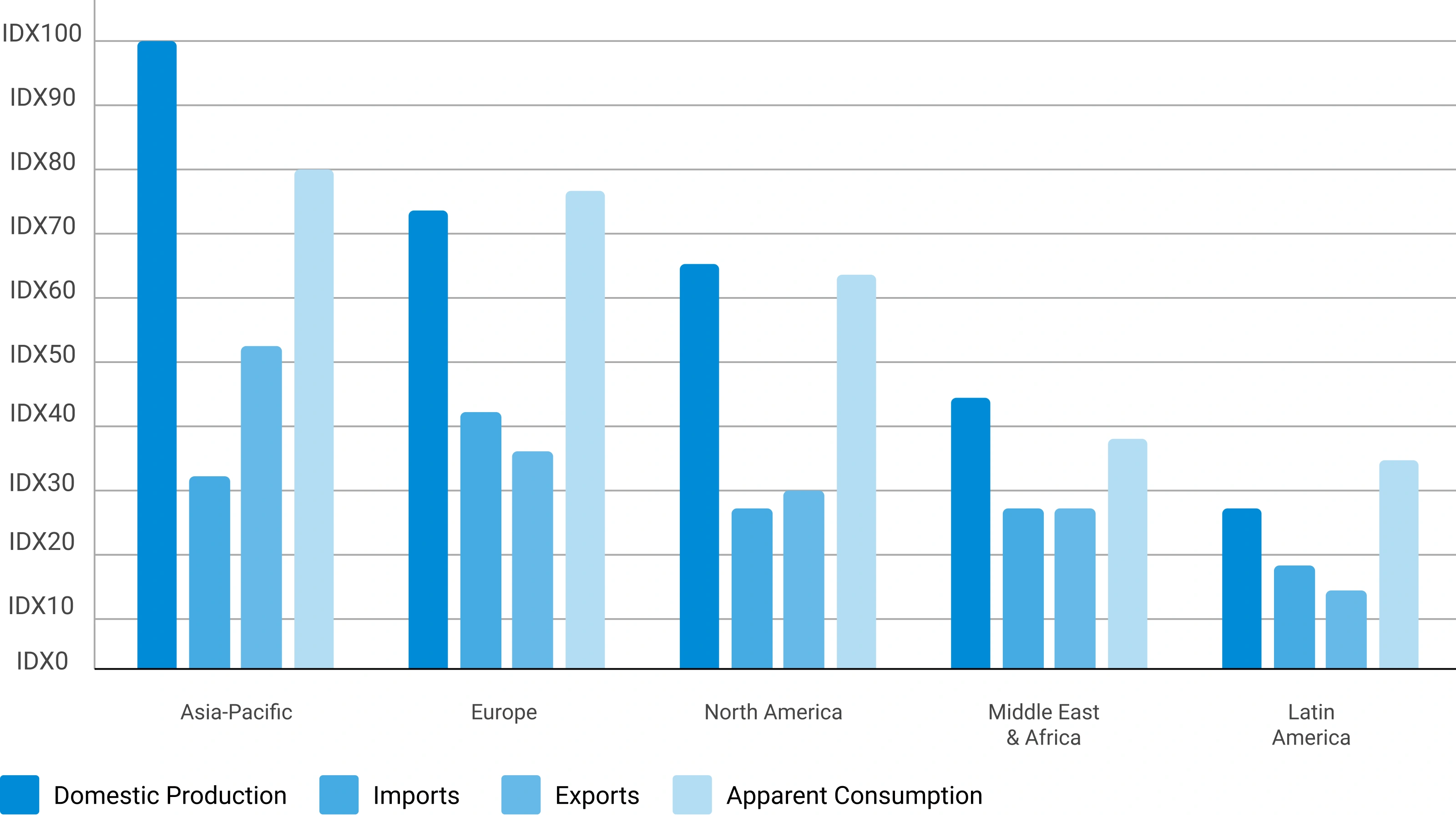
Apparent Consumption Model
Regional consumption is assessed using the standard apparent consumption formula:
Results identify net importing regions, net exporting regions, regional deficits, and surpluses — serving as an independent validation of supply and demand estimates.
Trade Flow Analysis — Net Supply Position by Region
Illustrative apparent consumption vs. domestic production across major regions — positive gap indicates net import dependency
Phase 5 — Primary Research: The Critical Validation Layer
Primary research tests and refines findings from secondary research through direct engagement with industry participants across the supply chain, demand side, and expert community. It captures intelligence that no database or published report can provide — the real-world experience of manufacturers, buyers, and specialists operating in the market.

Supply-Side Interviews
Conversations with chemical manufacturers, raw material suppliers, contract manufacturers, technology providers, and plant operators cover production trends, capacity utilization, pricing developments, technology shifts, and competitive dynamics.

Demand-Side Interviews
Engagement with OEMs, industrial consumers, procurement managers, distributors, formulators, and end-use manufacturers focuses on consumption trends, purchasing behavior, product substitution, demand outlook, and emerging applications.

Industry Expert Consultations
Additional interviews with industry consultants, independent experts, regulatory specialists, technical professionals, and research institutions provide deeper market context and validate key analytical assumptions.
Focus Areas of Primary Research:
Market Size & Forecast Validation
Revenue estimates, volume consumption, growth rates, forecast assumptions, regional demand.Supply Chain & Value Chain Assessment
Raw material sourcing, supply chain challenges, distribution networks, procurement practices.Production & Capacity Analysis
Manufacturing capacity, utilization rates, expansion projects, plant investments.Pricing & Cost Structure Analysis
Product pricing trends, feedstock costs, energy costs, margin pressures, pricing outlook.Competitive Landscape Assessment
Volume and value estimates confirmed to be fully consistent with one another before publicationInterview Volume by Market Scope
| Study Scope | Number of Interviews |
|---|---|
| Niche Market | 20 – 30 |
| Mid-Sized Market | 30 – 50 |
| Global Market | 50 – 80 |
| Highly Fragmented Market | 80 – 120 |
Interview Details:
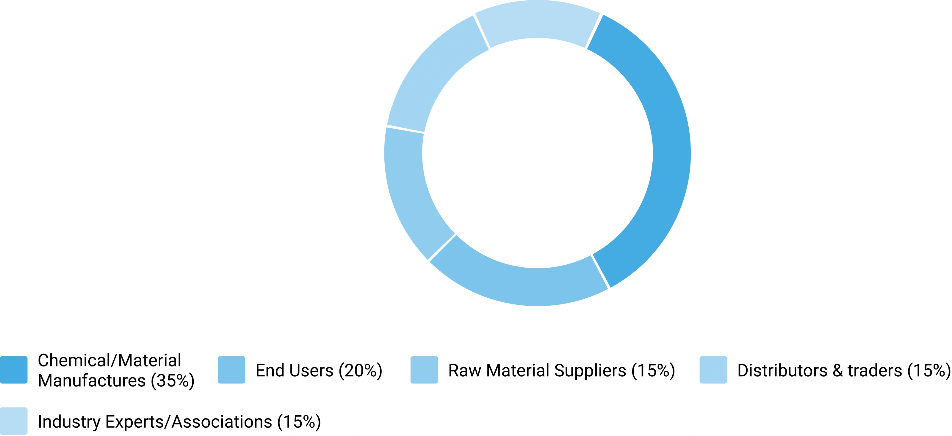
Category : Manufacturers, Suppliers, Distributors, End Users, Experts/Associations
Average Duration : 30–60 Minutes
Interview Mode : Video calls, telephonic interviews, expert consultations
Interview Format : Structured / Semi-Structured questionnaire
Focus Areas of Primary Research:
Market Size & Forecast Validation :
Revenue estimates, volume consumption, growth rates, forecast assumptions, regional demand.
Supply Chain & Value Chain Assessment :
Raw material sourcing, supply chain challenges, distribution networks, procurement practices.
Production & Capacity Analysis :
Manufacturing capacity, utilization rates, expansion projects, plant investments.
Pricing & Cost Structure Analysis :
Product pricing trends, feedstock costs, energy costs, margin pressures, pricing outlook.
Competitive Landscape Assessment :
Market share, competitor positioning, strategic initiatives, partnerships, acquisitions.
Primary Research — Stakeholder Coverage by Category
Distribution of interview respondents across stakeholder categories (% share from PPT data)
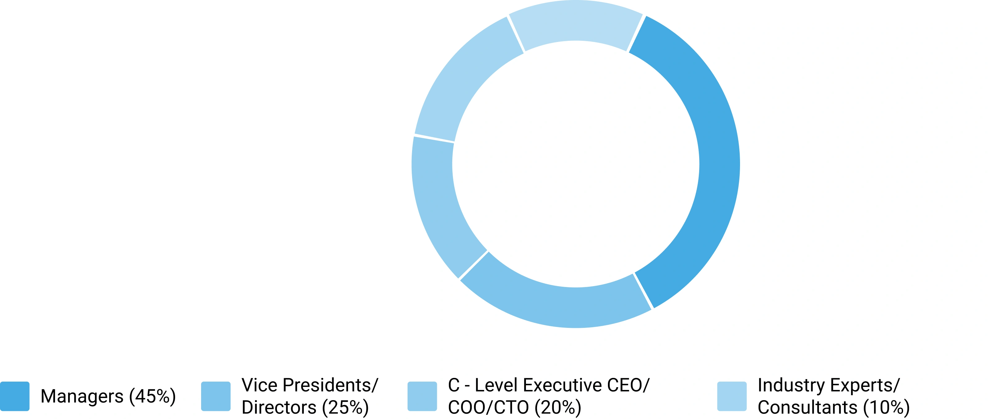
Primary Research — Respondent Designation Profile
Seniority breakdown of interview respondents (% share from PPT data)
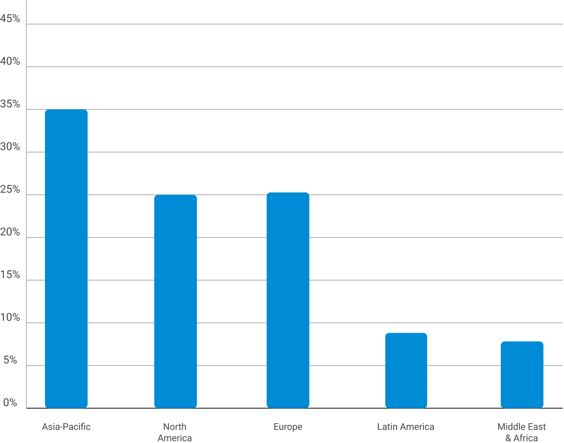
Primary Research — Geographic Coverage of Interviews
Regional distribution of primary research engagement (% share from PPT data)
Phase 6 — Data Triangulation and Market Validation
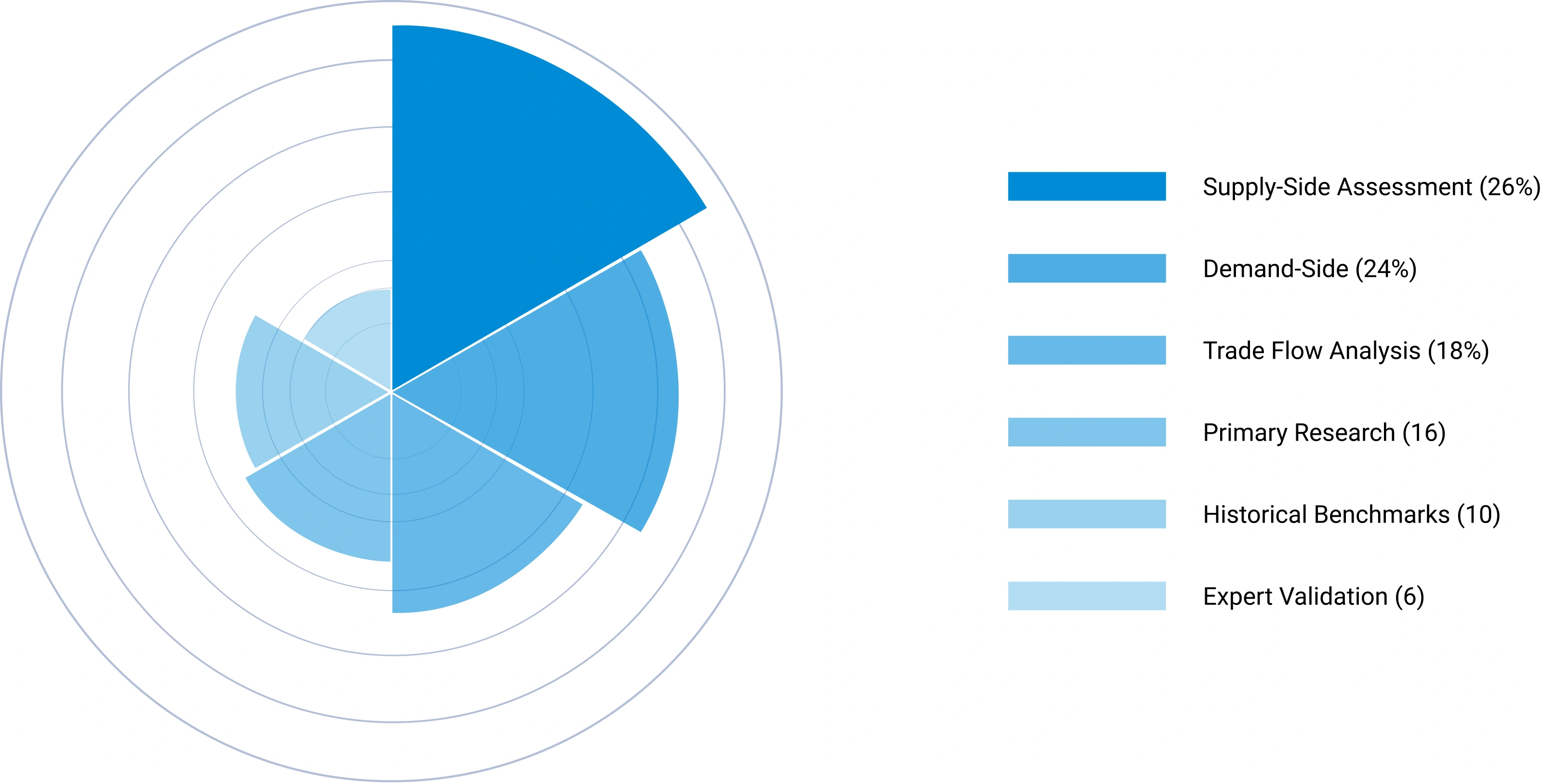
No single methodology is relied upon in isolation. Multiple independent estimation approaches are combined and reconciled to ensure consistency, accuracy, and analytical defensibility. Any material deviations between approaches are investigated and adjusted through additional validation cycles.
The final market size is derived through weighted triangulation of all validated methodologies. Any material deviations between approaches are investigated and adjusted through additional validation cycles. The outcome represents the most realistic assessment of the market based on available evidence and expert confirmation ensuring that volume and value estimates are fully consistent with one another.
Triangulation Framework — Input Contribution Weight
Relative weight each sizing input contributes to the final reconciled market estimate
Phase 7 — Forecast Modeling: Projecting Future Market Evolution
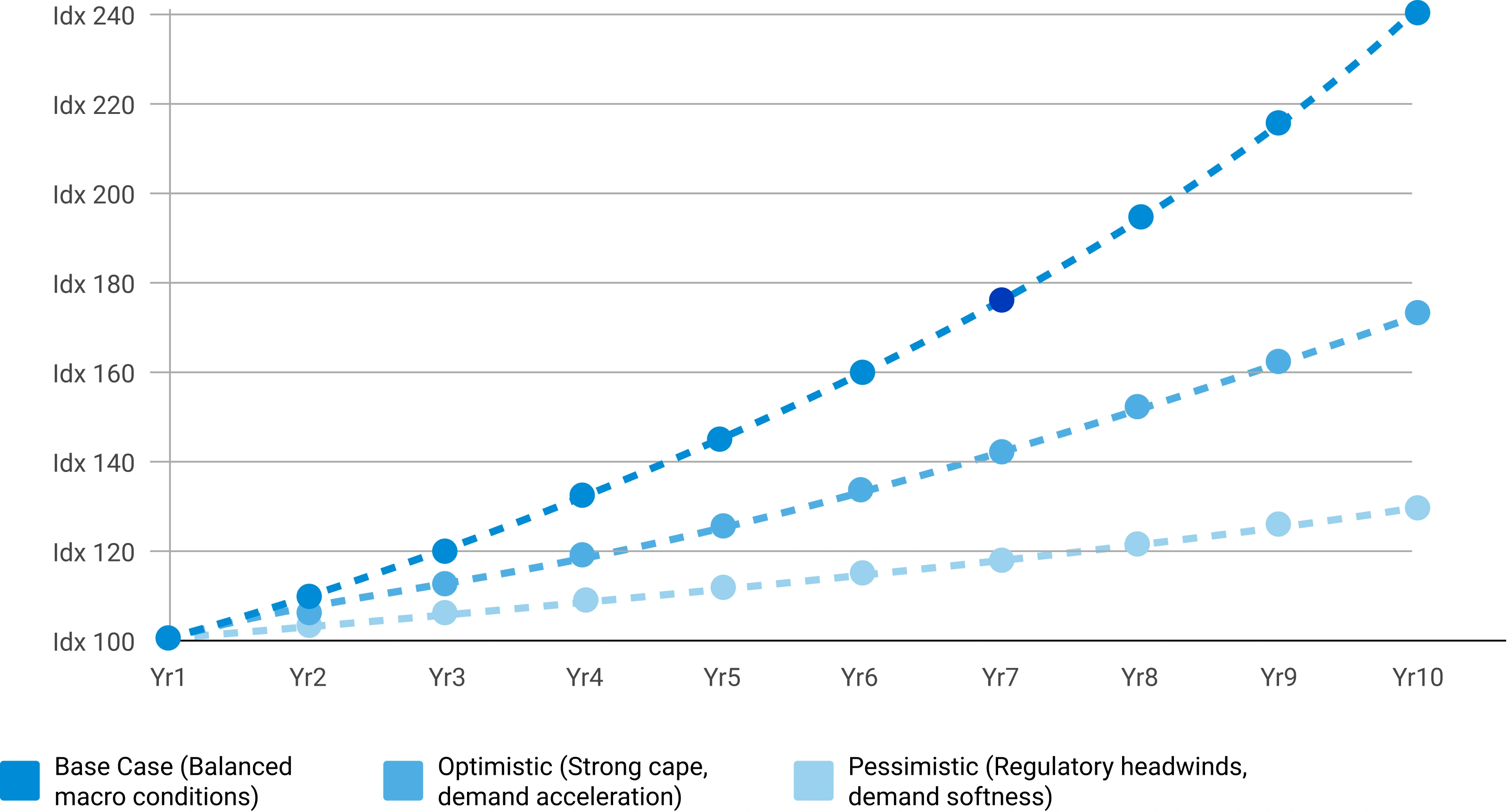
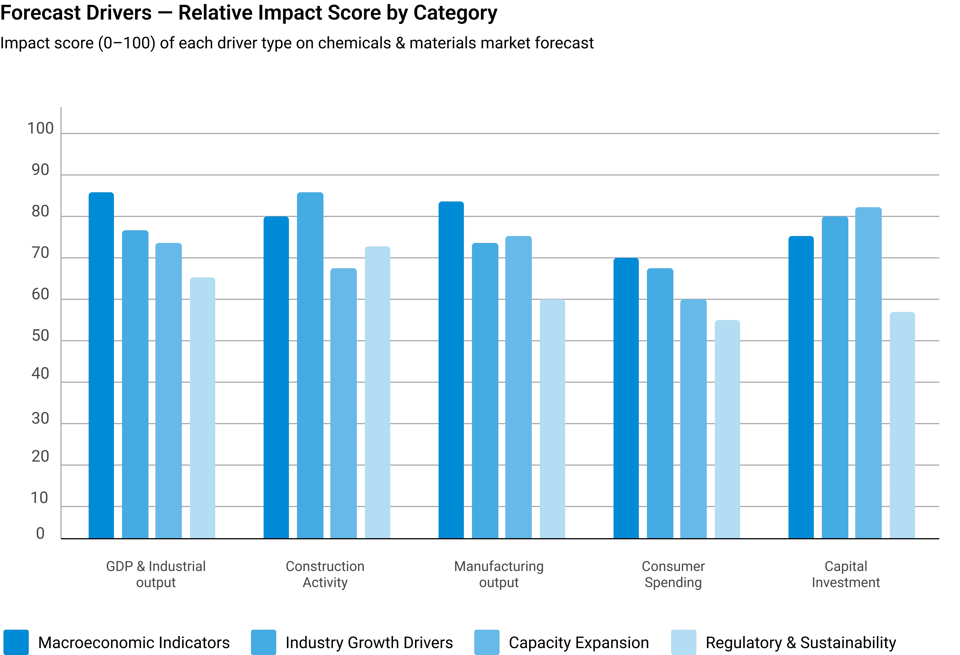
Forecasting evaluates the future trajectory of the market using a combination of quantitative indicators and qualitative assessments across economic, industry, and regulatory dimensions. Rather than simple extrapolation, each driver is independently modeled and integrated into a composite forecast.
Macroeconomic Indicators
GDP growth, industrial production, manufacturing output, construction activity, consumer spending, and capital investment form the quantitative foundation of long-term demand projections. These are applied at country, regional, and global levels.
Industry Growth Drivers
Urbanization, infrastructure development, industrialization, technological innovation, sustainability initiatives, and evolving product performance requirements are assessed at regional and industry levels — capturing both structural and cyclical demand drivers.
Capacity Expansion Analysis
Announced plant expansions, new manufacturing facilities, technology upgrades, and strategic investments are evaluated to determine future supply-demand dynamics and potential market tightness or oversupply situations.
Regulatory & Sustainability
Environmental regulations, chemical safety standards, emission reduction targets, circular economy initiatives, and sustainability requirements are incorporated as they often influence product adoption rates and market growth trajectories.
Scenario Forecast Range — Indexed Market Growth (Year 1–10)
Illustrative indexed growth trajectories across Base, Optimistic, and Pessimistic scenarios over a 10-year forecast horizon
Forecast Drivers — Relative Impact Score by Category
Impact score (0–100) of each driver type on chemicals & materials market forecast



Comments
Share your thoughts, ask a question, or provide feedback about this report.